Layout Driver Power MICRO V2 BY R2R PCB Design: Expert Tips for Optimal Performance! Maximizing signal integrity with ground plane pcb design
So, you think you're ready to dance with the GHz? You're dreaming of a PCB so sprightly, so responsive, it makes lightning look like a snail on molasses? Well, buckle up, buttercup, because designing a high-frequency PCB is less "easy bake oven" and more "nuclear fusion." Let's be honest, most of us are just trying to avoid turning our prototypes into fancy paperweights that smell vaguely of burnt toast and regret.
High-Frequency PCB Design Tips: Because Apparently, Magic Isn't Real

The first image suggests someone named Frank has tips. Bless Frank's heart. And bless anyone who thinks a single PowerPoint slide will magically imbue them with the arcane knowledge needed to tame the unruly beast that is signal integrity. The truth is, high-frequency design is like trying to herd cats... made of electricity... that are allergic to right angles. It's all about impedance matching, minimizing parasitics, and generally praying to whatever silicon deity you hold dearest. Good luck with that.
One crucial aspect they usually omit is the existential dread that accompanies staring at simulation results that look like a Jackson Pollock painting, but instead of being a masterpiece, it's just a screaming indication of a design flaw. You'll question your life choices. You'll wonder if you should have become a baker. You'll briefly consider a career change involving goats and a remote mountain cabin. But you'll persevere. Probably. Maybe. No promises.
Power Supply PCB Design: The Unsung Hero of "Don't Blow Up My Stuff"

Ah, the power supply. The Rodney Dangerfield of PCB design. It gets no respect, but without it, absolutely nothing works. It's the unsung hero quietly providing the juice for all your fancy microcontrollers and high-speed data lines to do their thing. Think of it as the PCB's liver – essential, but nobody wants to talk about it.
Now, let's talk about layout. Star grounding. Plane layers. Clearance. Thermal management. These aren't just buzzwords; they're the commandments etched onto the silicon tablets of power supply design. Ignore them at your peril. Your circuit will reward your hubris with a spectacular display of sparks, smoke, and possibly a small fire. It's a learning experience, really, albeit one that involves a significant amount of swearing and a hefty bill for replacement components.
Ultimately, designing any PCB, especially one dealing with high frequencies or significant power, is a delicate dance. It's a battle against physics, a wrestling match with electrons, and a constant test of your sanity. So, arm yourself with knowledge, a healthy dose of skepticism, and maybe a fire extinguisher. You're going to need it.
If you are searching about LAYOUT DRIVER MICRO BOOSTRAP PDF you've came to the right web. We have 25 Pics about LAYOUT DRIVER MICRO BOOSTRAP PDF like Mastering PCB Layout Design Rules for Optimal Circuit Performance - 86PCB, PPT - Tips to design High Frequency PCB for optimal performance Frank and also R2R Network PCB 1.0 - EasyEDA. Here it is:
LAYOUT DRIVER MICRO BOOSTRAP PDF
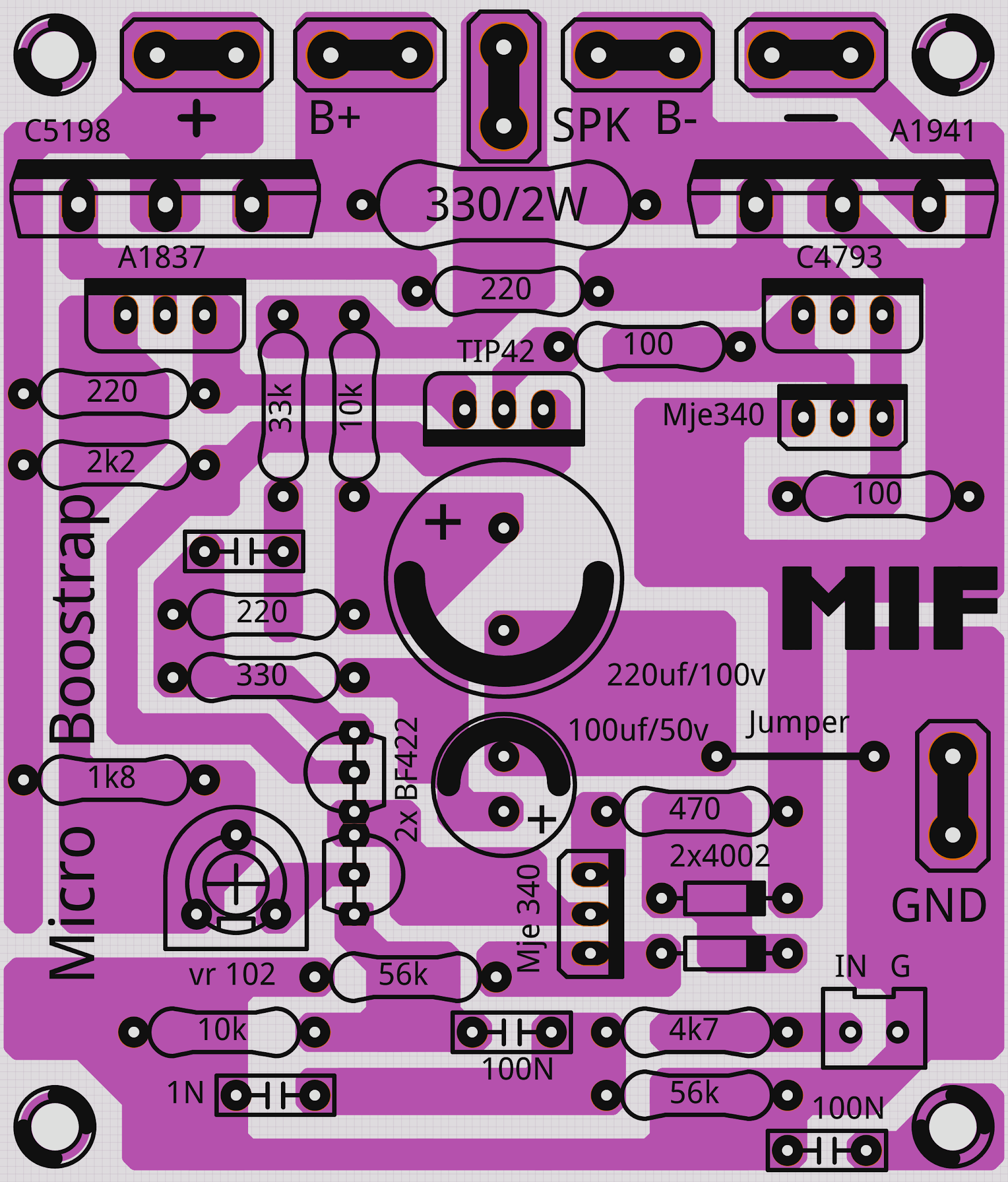 miflayout.blogspot.com
 LAYOUT DRIVER NKRI GB DINA
 miflayout.blogspot.com
 Layout Driver TBM
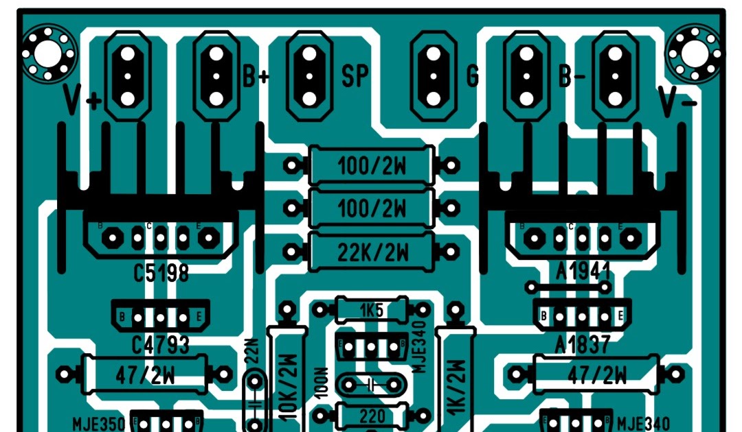 miflayout.blogspot.com
 77+ Baru Layout Driver Micro Bostrap Tef, Skema Power
 superpowert.blogspot.com
 3D Curve Of The Design Expert Program Prediction 7.0 Optimal Point
 www.researchgate.net
 77+ Baru Layout Driver Micro Bostrap Tef, Skema Power
 superpowert.blogspot.com
 Layout Driver Micro By Askar Pcb - Gudang Skema
 gudang-skema.blogspot.com
 micro pcb askar
Power Supply PCB Design Guidelines For Manufacturing - VSE
www.vse.com pcb guidelines vse
Layout Driver TBM
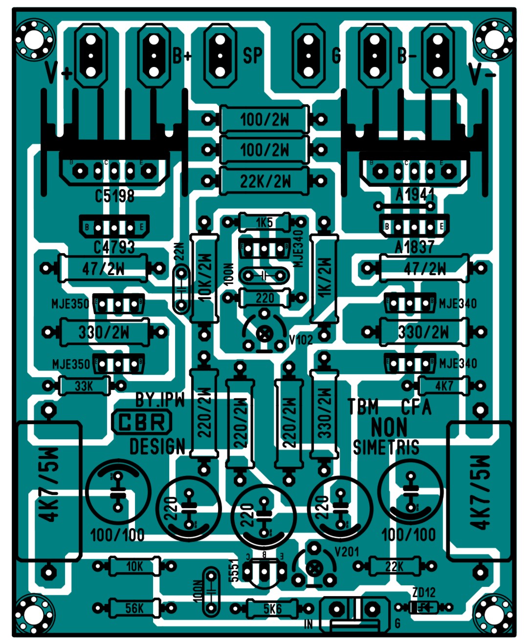 miflayout.blogspot.com
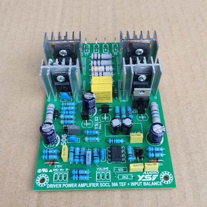
 Perbedaan Ocl Dengan Socl Pcb Layout Socl Boom Tef Dr - Vrogue.co
 www.vrogue.co
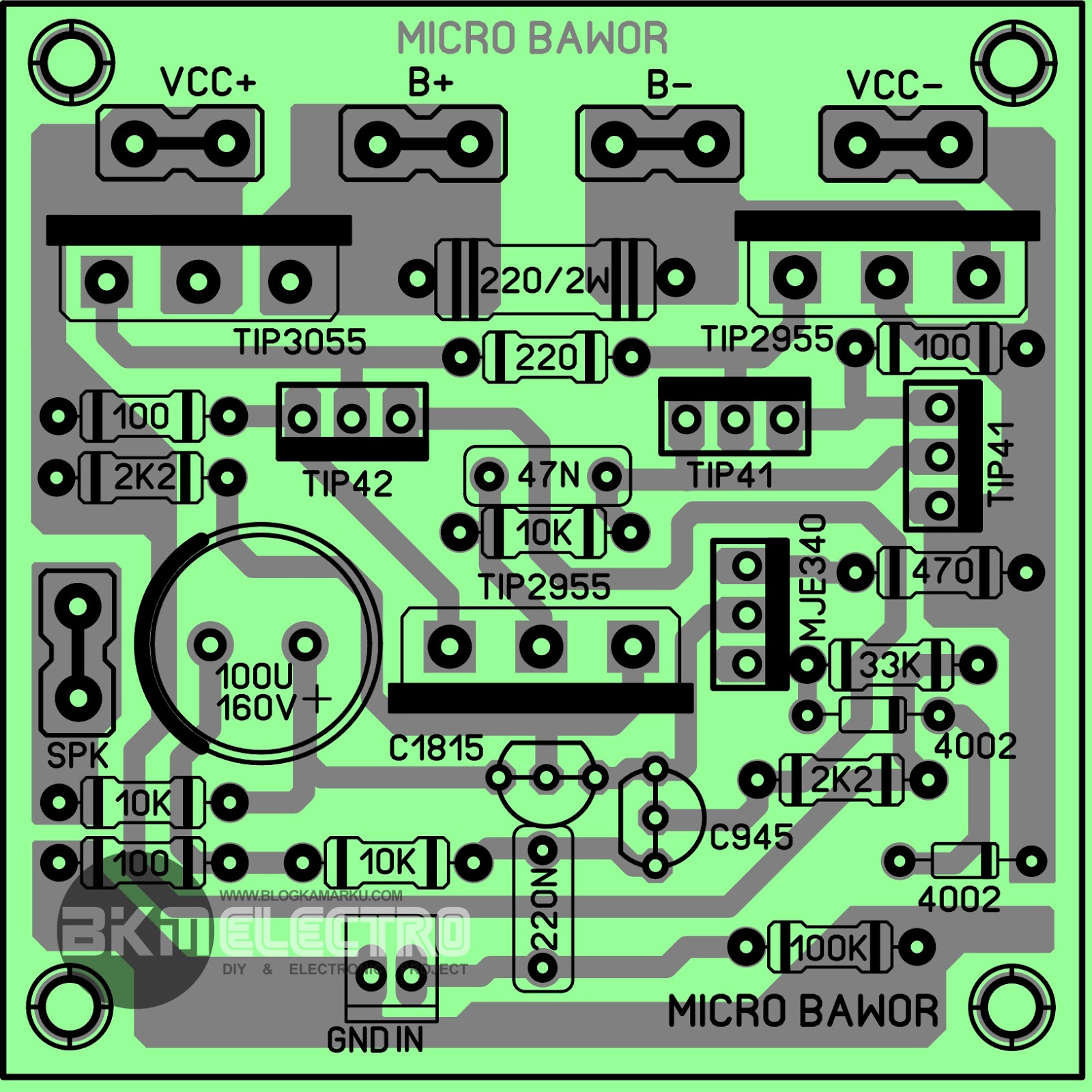
 Layout PCB MCRO BAWOR STANDARD Driver Amplifier – BLOGKAMARKU
 blogkamarku.blogspot.com
 driver pcb amplifier bawor mcro blogkamarku
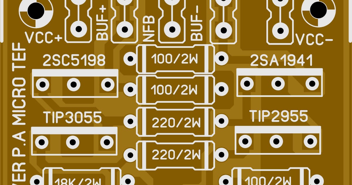
77+ Baru Layout Driver Micro Bostrap Tef, Skema Power
 superpowert.blogspot.com
 Layout Driver Tbm Dual Input Beserta Pengertian Nya – Artofit
 www.artofit.org
 Maximizing Signal Integrity With Ground Plane PCB Design - Expert Tips
 www.pcba-manufacturers.com
 Layout Driver Tbm Dual Input Beserta Pengertian Nya – Artofit
 www.artofit.org
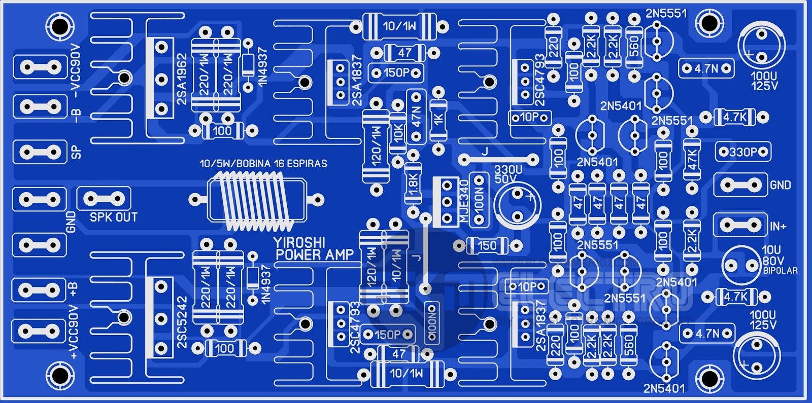
 PCB Layout Yiroshi Driver Power Untuk Lapangan – BLOGKAMARKU
 blogkamarku.blogspot.com
 pcb lapangan
PCB Design: Benefits Of Collaboration | Solid Edge
 solidedge.siemens.com
 pcb collaboration siemens edge benefits solidedge
PPT - Tips To Design High Frequency PCB For Optimal Performance Frank
www.slideserve.com Layout Driver Power Amplifier: Optimal Design Techniques For High
 hillmancurtis.com
 Skema Driver Micro Mungil V2 & M2 | Thicke.net
 thicke.net
 77+ Baru Layout Driver Micro Bostrap Tef, Skema Power
 superpowert.blogspot.com
 Layout Driver TBM Dual Input: Pengertian Dan Layout
 in.pinterest.com
 Layout Driver Micro V2 - Artsied
 artsied.blogspot.com
 Mastering PCB Layout Design Rules For Optimal Circuit Performance - 86PCB
 86pcb.com
 R2R Network PCB 1.0 - EasyEDA
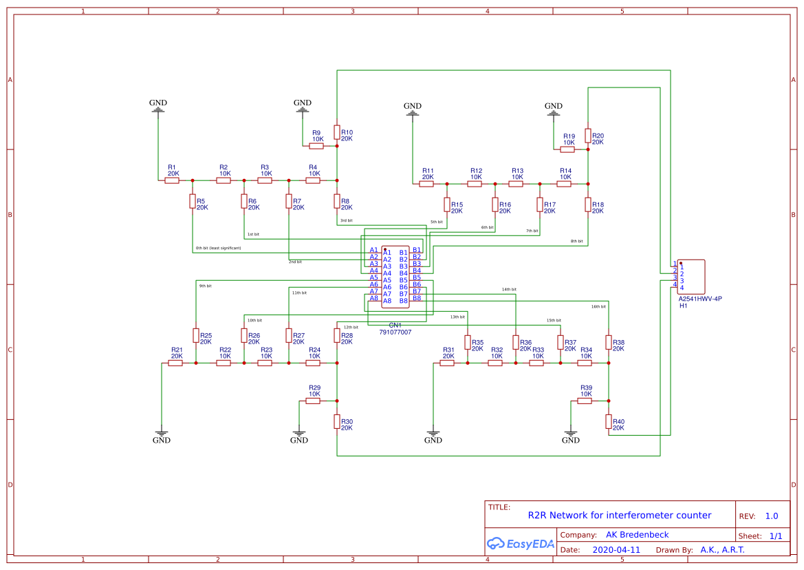 easyeda.com
 pcb r2r network easyeda 2020
Micro pcb askar. Layout driver nkri gb dina. 77+ baru layout driver micro bostrap tef, skema power